CCD Board Designs
Power Monitor Board, ![]() EL-1198
EL-1198
SCHEMATIC: boards/EL1198/Monpwr3.sch.pdf
The Power Monitor card is used in most of the UCO/Lick Observatory CCD Controllers. It monitors the voltage levels of the power supplies, the AC voltage level and accepts inputs from the SDSU Utility board and front panel switches. Using these inputs an Altera programmable logic chip determines if the +16V, -16V, and +38V supplies may be supplied to the VME style backplane and in what order. The idea is to allow the +/-16V to be supplied to the backplane only if all of the voltages are above a predetermined level, the Utility board program is ready for them, and the front panel switch is set to on. The 38V to the backplane will only be supplied if the above conditions are true and the 16V supplies are already enabled. The Altera chip incorporated a delay between when the 16V is enabled and the 38V is enabled.
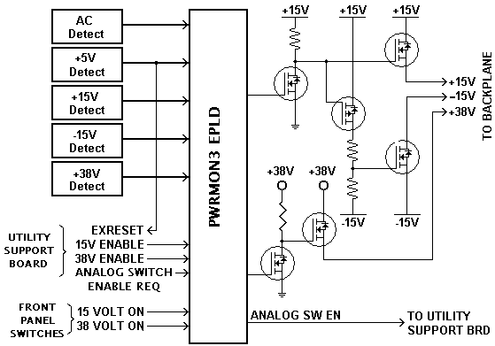
The 16V and 38V supplies are used to supply the DACs on the SDSU Analog board that supply bias voltages and clock waveforms to the CCD. Because of this we want the 16V and 38V supplies held off until the programming can setup the DACs and thus keep spurious voltages off of the CCD chip. As the block diagram indicates, the Altera chip provides the logic functions for the board. It contains the coding 'monpwr3'. It should be noted that the voltage sensors that are used only sense voltages lower than a set point and do not give an indication of an over voltage condition.
Detailed description:
120V AC is applied to pins 1 and 7 of the input connector J1 and from there to pins 1 and 4 of the HCPL3700 optocoupler through R1-R2 and R3-R4. These resistors set the turn on point of the optocoupler to be about 108V AC. Thus if the line voltage falls below this point the normally low output of the chip will go high signaling a failure of the AC line. U2, a TL7705A Supply Voltage Supervisor, has its sense input tied to the 5 volt supply via a 100 ohm resistor. In this configuration the output will become active (low) if the input drops below 4.55-4.6 volts. Its output is also sent back to the Utility board as the EXRESET, external reset, signal to the SDSU system. U3 is a TL7715A which is a 15 volt version of the TL77xx. It's threshold is set to 13.8 volts by internal resistors. U4 is another TL7715A but it has it's ground input set to -16V and it's sense input tied to ground so that it can sense the negative voltage. The threshold is now -13.8 volts. The generic version, TL7702A, is used to sense the +38V supply by using a voltage divider at the input. If the voltage at the sense input goes below 2.5 volts the output will become active.
Besides the inputs from the voltage sensors, the circuit accepts logic inputs from the Utility board. These come in on J2 and are comprised of '15V ENABLE', '38V ENABLE', and 'ANALOG_SW_EN_REQ'. These are all fed directly into the Altera chip on pins 10, 60, and 13 respectively. Also, the RESET output of the 5V-supervisor chip is fed back to the Utility board as EXRESET, the external reset. Note: for test purposes, a test connector with pins 5, 6, 7, & 8 shorted can be connected to J2 to eliminate the need for having a working Utility board during testing. The board also receives inputs from the front panel enable switches MAN 15V ON and MAN 38V ON via J3. These switches are used for local control of the voltages to the controller backplane. Logic in the EPLD ensures that the front panel switches can only turn on the power supplies if the software has already enabled them. Thus, both the software and the front panel switches must be set to get the power applied to the backplane. Also, a shorting block, W1, is provided for backwards compatibility with older controllers that don't use the control bit for enabling the analog switches in the CCD electronics box.
G7, an LM555 timer, provides a 100KHz clock to the clock input of the Altera chip. The EPLD uses this as a time base to determine the various delays within the chip. These are seen as the delay between the turn on of the 16V supplies and the 38V supply and the delay needed for recovery of the 16V supply from the current inrush when the MOSFET turns on. The Altera chip 'monpwr3' provides the logic to determine the states of its three output pins. The outputs are 15ON, 38ON, and ANA_SW_ENABLE. The 15V ON signal turns on MOSFET Q2 which in turn turns on Q4 which passes the +15 volt supply to pin 6 of J6 and on to the backplane. In a similar manner, when Q2 turns on, Q7 also turns on. This causes MOSFET Q6 to turn on and pass the -16V supply to pin 8 of J6. The 38ON signal and MOSFETs Q3 and Q5 work in a similar fashion. The last output of the EPLD is the ANALOG_SW_EN. The logic of the EPLD only allows this output to go high if both the ON15 and ON38 are enabled.
EPLD description:
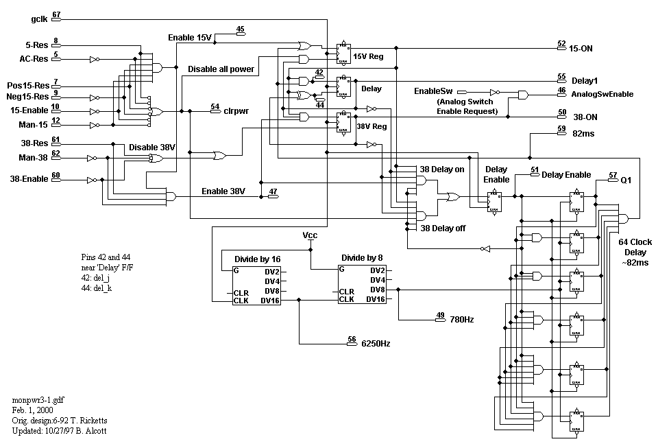
Power Monitor EPLD - monpwr3
The Altera EPLD used on this board is an EPM7064LC68. This device has 64 macrocells, 48 I/O pins, and 1,200 usable gates. The chip can be programmed with the proper hardware and easily erased with a UV source. We have used both hardware and software from Altera. The schematic, timing diagram, and project report has been provided with the Power Monitor schematic.
At the top of the drawing is the input for the 100KHz on pin 67. This clock provides all of the timing functions. At the top center of the diagram are three JK flip-flops. Two of these are the output control registers for the power supply enables. Output pin 52 (top flip-flop) will, if high, enable the +/- 16V supplies. Pin 50 (bottom flip-flop) will, if high, enable the 38V supply. The center flip-flop allows the delay counter to start. The purpose of the delay is to control the sequence of that application of power. We want the +/-16V supply to come on before the +38V supply. This will insure that the DACs on the SDSU clock board will have power before the voltage that they control is present. This will prevent dangerous, uncontrolled voltages from being applied to the CCD. When the power is being shut down we also want to sequence the power supplies such that the +38V is removed before the +/-16V is removed. An 'and' gate at the output of the 38-ON is used to ensure that the analog switches in the dewar electronics box will not come on unless the voltages to the DACs is applied properly.
The six input 'and' gate at the top left of the diagram controls the enabling of the +/-16 volts. It will be enabled if the +5V, +/-16V, and AC line are within the proper range; the signal from the front panel toggle switch is present, and the enable from the SDSU Utility board is present. If these conditions are met the '15-ON' flip-flop will be set, and will enable the +/-16V to be applied to the backplane.
The output of the 'and' gate is also routed to a 4 input 'and' gate at the bottom of the left-hand edge of the diagram. This gate will be enabled if all of the conditions for the +/-16V, the +38V supply is in proper range, and the enable signal from the front panel switch is present, and the Utility board enable is present. At this point a sequence of events will occur. A 3 input 'and' gate leading to the 'J' input of the ON-38 flip-flop will have two of its inputs enabled. The third input comes from the 'delay' flip-flop that will not yet be set. In the center of the sheet are two 6 input 'and' gates. The top one, labeled '38 Delay on' will now be enabled. The next clock cycle will set the 'Delay Enable' flip-flop. This will, via the inverter, disable the input so it will not continue to be set and will enable the six bit counter. When all six bits of the counter are high the 'Delay Enable' flip-flop will be reset and the 'Delay' flip-flop will be set. This will happen after 64 clock cycles or about 82 milliseconds. The two frequency dividers in the center of the page have been added to lengthen the delay time from the original 0.7 milliseconds to approximately 82 milliseconds. This provides ample time to allow for the momentary spike on the +16V supply due to the current in rush at turn on. When the 'Delay' flip-flop is set the '38-ON' flip-flop will be enabled and will clock high on the next clock. The output of the '38-ON' flip-flop will cause the 'Delay' flip-flop to be reset on the next clock.
All of the of the inputs to the input to the 'Enable-15' 'and' gate are also sent to a six input 'nor' gate. If any of these signals are absent the gate will produce the 'clrpwr' signal on pin 5. This signal is routed to a two-input 'or' gate. The other input to the 'or' gate comes from a three input 'nor' gate tied to the three enable lines for the +38V. If any of these enable signals are not present the two input 'or' gate will cause the '38-ON' flip-flop to be reset. Then the six input 'and' gate labeled '38 Delay off' will be enabled causing the delay cycle to start. At the end of the 64 clock cycles the 'Delay' flip-flop will be set. This will cause the '15-ON' flip-flop to be reset on the next clock if the delay was caused by the 'clrpwr' signal. A loss of the 38V alone will not reset the flip-flop. The 'Delay' flip-flop will be cleared when the other two flip-flops are either both set or both reset.